

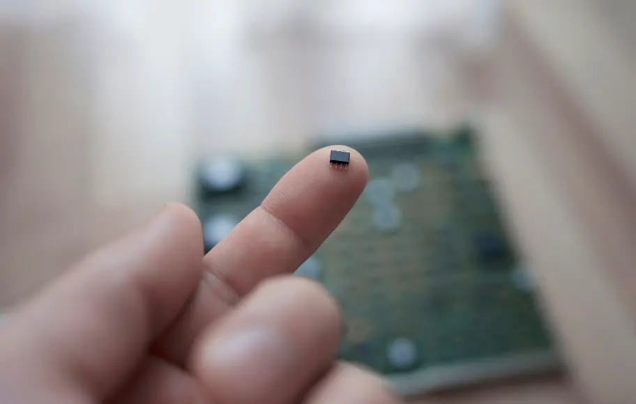
As quantum computing moves from theoretical promise to real-world engineering, one principle is becoming clear. The future of this technology will not be won through miniaturization alone. Unlike classical semiconductor devices that thrived on shrinking feature sizes, quantum systems depend on structural precision, alignment accuracy, and environmental stability. Erik Hosler, a panelist focused on quantum-scale lithographic challenges, emphasized this point during the SPIE Advanced Lithography symposium by noting the vital role of precision.
Quantum devices rely on interactions that are inherently sensitive to spatial variation and material defects. Whether using superconducting loops, trapped ions, or photonic circuits, the function of a qubit often depends on exact placement and undistorted interfaces. Variability, once tolerable in some classical systems, can become a fatal flaw in quantum designs. It places pressure on patterning tools, resist materials, and process controls to deliver not just smaller, but more consistent and tunable structures.
Accuracy as the Driving Metric
In lithography for classical logic, success was measured by how tightly designers could pack transistors together. Shrinking node sizes led to more transistors per chip, more power, and faster operation. But in quantum hardware, that formula does not always apply. Packing more qubits into a smaller area introduces crosstalk, thermal stress, and fabrication yield problems. Instead, the emphasis shifts to the repeatability of placement and the fidelity of pattern transfer.
Errors introduced during fabrication directly affect qubit performance. A waveguide etched too wide may leak photons. A Josephson junction misaligned by even a few nanometers may exhibit unexpected tunneling behavior. Each of these issues can compromise the delicate quantum states that drive computation.
That is why so much effort at the SPIE conference is centered on reducing line edge roughness, improving resist profiles, and enhancing metrology. Patterning errors are not just defects. They are sources of decoherence. They limit the effective lifetime of qubits and increase the burden on error correction.
Chasing Perfection with the Right Tools
At the panel, the importance of this precision was framed with a mixture of realism and ambition.
“We’d like to see perfection in our patterning, but we’ll settle for striving for perfection,” Erik Hosler shares. This comment reflects the ongoing tension in quantum fabrication. On one hand, the ideal is to create features with atomic precision, zero roughness, and complete dimensional control. On the other hand, every lithography and etch step involves tradeoffs. Mask variation, etch loading, and stochastics from resist chemistry all introduce noise.
The goal, then, becomes narrowing the range of deviation. Patterning systems must be evaluated not just on resolution, but on uniformity and repeatability. Process windows must shrink. In some cases, it is better to have slightly larger features that are always consistent than to push to the physical limits and introduce variability.
Advanced EUV and multicolor lithography may offer part of the solution. By enabling better control over exposure conditions, these tools give engineers more degrees of freedom to tune pattern profiles. But hardware alone is not enough. Data-driven process control, using in-line metrology and real-time correction, is becoming critical. Quantum hardware teams are beginning to adopt feedback-driven fabrication methods pioneered in classical fabs, but with even tighter tolerance thresholds.
Impacts on Qubit Design and Packaging
Precision patterning affects more than qubit formation. It also shapes how systems are routed, packaged, and integrated. For instance, photonic qubits rely on grating couplers, beam splitters, and delay lines. Each of these must be fabricated with tight control over depth, width, and angle. Variations in any one of these parameters can shift optical phase or introduce loss.
In superconducting systems, wiring paths must be isolated and impedance matched. Variations in trace width or dielectric spacing change signal behavior. These issues are compounded when multiple layers are involved, especially if features span both classical control circuitry and quantum cores.
Packaging becomes another point of constraint. Flip-chip bonding, wafer-scale integration, and 3D stacking must all preserve alignment across thermal cycles and prevent mechanical drift. It introduces demand for materials and adhesives that do not shrink, warp, or shift under changing temperature and humidity.
As systems move toward higher density and larger scale, the importance of patterning uniformity increases. Yield losses in classical systems are tolerated by redundancy. In quantum, where each qubit may require thousands of physical components and contribute to system-wide coherence, one flawed element can degrade the entire machine.
Rethinking Design for Manufacturability
Precision demands are often pushed against standard design practices. Many early quantum devices were hand-tuned in the lab, with generous feature spacing and custom wiring. These prototypes were useful for exploring physics but not for scaling production. Moving to a manufacturable system means constraining layouts, using standard layers, and adopting Design-For-Manufacturing (DFM) principles.
Engineers must balance the physical demands of quantum operation with the practical limits of patterning. That means simplifying routing, minimizing layer transitions, and ensuring that each feature aligns with known process capabilities. Tools like layout-aware simulation and pattern fidelity modeling become essential.
Collaborations between fab engineers and quantum physicists are essential here. Without feedback between design and process teams, even the best-intentioned architecture may be impossible to build. That is why so many SPIE sessions stress cross-disciplinary knowledge and iterative co-design.
Where Precision Leads
The shift from miniaturization to precision reshapes how the quantum industry thinks about progress. The question is no longer how small we can make a feature, but how predictably we can make it. It leads to new research into low-variability resists, post-etch smoothing, and lithographic compensation techniques.
It also opens the door to smarter layout strategies. Instead of treating lithography as a post-design constraint, engineers are beginning to co-optimize placement with exposure. Adjusting feature shapes to account for diffraction, proximity, and etch behavior allows for cleaner results at scale.
It is not just a theoretical shift. It has tangible impacts on build time, yield, and system performance. With fewer rework cycles and more predictable results, quantum hardware becomes easier to integrate and deploy. The manufacturing stack becomes more agile, and the transition from prototype to product accelerates.
A Future Built on Stability
The quantum hardware of the future will be defined not by its minimum feature size but by its stability and repeatability. Engineers will prioritize processes that create qubits and circuits that function consistently over time. This approach leads to machines that are easier to calibrate, simpler to repair, and more likely to perform well under real-world conditions.
Precision is the new frontier. It demands better tools, tighter process windows, and smarter design. But it offers a path to scalable, manufacturable quantum systems. The goal is not just to push the limits of physics, but to do so with control.
Quantum computing does not need to be perfect to be useful. But it needs to be precise enough to be reliable. And that reliability begins with how well we pattern the building blocks.
Comments are closed.